SMD elements expanding a greater thickness and parts on the motherboard. The PCB stencil soldering procedure does not influence making use of a soldering wave, even in a reflow oven or making use of vapor phase soldering. The possible tin solder is loosened up in the form of a paste using a stencil and also squeegee. The parts are after that noted on the solder paste. The sticky pressure of the paste avoids it from diminishing. Larger parts are typically Glued to it.
SMD Assembly
MOKO Printed Circuit Board Assembly Offers thorough solutions for putting together surface-mounted (SMD) parts and also parts for push-through setting up (THT). Our production center is technologically flexible, we tackle the setting up of numerous components from the SMD elements of dimension 0201 to the integrated circuits with QFP and also BGA & uBGA real estates in outstanding top quality with a lot of experience. Our regular collection dimension is in between 1 and also 1000 items, the regular order duration is 5 to 10 days.
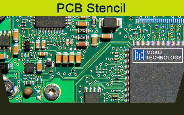
SMD assembly PCB stencil
Develop solder paste PCB stencil
9 Action:
Step 1: Product and also prep work
Step 2: Prepare the PCB format and also identify dimensions
Step 3: Produce Gerber data
Step 4: Open Gerber file for conversion
Tip 5: Export Gerber to SVG file
Action 6: Cutting software program
Action 7: Modification The dimension of the style
Tip 8: Prepare openness and also equipment
Step 9: Cut your pattern
Utilize a Cricut cutting maker and also Sure-Cuts-A-Lot software program to develop usable solder paste stencils for digital prototyping purposes.
The high quality as well as precision of the patterns acquired are good enough, size 0805 and also TQFP (0.8 mm pitch) digital component prototype.
This Instructable on a tutorial I originally wrote based upon solder paste stencils.
I would certainly not recommend buying a Cricut simply to create solder paste stencils. Nevertheless, if you have a friend or relative that owns one, or at a Cricut shop or at the flea market, then acquiring Sure-Cuts-A-Lot software will certainly transform a Cricut right into an extremely valuable gadget. Performance after that comes to be something like a low-end vinyl/craft cutter like its Craft Robo.
Action 1: Product and also prep work for PCB stencil
Products
-- Cricut device
-- Sure-Cuts-A-Lot software
-- Gerber audience software application
-- Transparencies for overhead projectors that you can purchase any workplace supply store
-- A Windows XP/ View computer
Prep work
Your Cricut needs to have a particular firmware variation. You can update/downgrade the firmware by downloading and install Cricut Layout Workshop and complying with the guidelines under Aid to update the firmware. See the Sure-Cuts-A-Lot FAQ to find out more.
Step 2: Prepare the PCB format and also establish dimensions
It can take some trial and error to develop respectable solder paste PCB patterns is not very precise. It reduces rounded sides as well as disregards shapes smaller than concerning 18mil (0.46 mm) by 50mil (1.27 mm). That said, you ought to make sure that every one of your element pads are big than these. To ensure a pad still has adequate solder paste area, make the pad a lot more. The KiCAD EDA Collection PCB layout program has the ability to alter all one impact pads at a time. Solder has this remarkable home that links to metal parts when reflow discovers. As long as your PCB has accurate solder stand up to, solder metal pieces will be found to web link. So do not be also worried regarding pads (primarily claim +/- 20%).
You require the specific measurements of your PCB template for later. Use your PCB design software distance device to determine the distance between the outermost element pads. Not the size of the PCB, but the range between outer pad edges. In the example listed below, the PCB has a size of 2.3 ", but the edge to border pad distance is 2.142".
You can determine ranges by selecting illustrations from the layer pull-down menu as well as clicking the Capacities button in the right tool food selection. It's the 4th button from the bottom.
Step 3: Producing Gerber documents
Attract your PCB format making use of the Gerber solder paste stencil.
When utilizing KiCAD, select Draw from the Data menu. In the plot home window, pick SoldP_Cmp for the solder paste component layer as well as click the Story button.
Step 4: Open Gerber apply for conversion
Open up the documents in Gerber Customer. Select Open Layer (s) from the Data menu.
Tip 5: Export Gerber to SVG file
After that export the documents in SVG layout. Select Export, after that SVG ... from the File food selection.
Action 6: Cutting software
Produce solder paste patterns with Cricut
Import the SVG data right into Sure-Cuts-A-Lot by selecting Import SVG ... from the Data menu.
Step 7: Resize the design
Produce solder paste stencils with Cricut
Click Maintain Percentages in the Feature home window as well as set the pattern's size to the worth formerly kept in mind.
Tip 8: prepare openness and maker
Create solder paste stencils with Cricut
Take a sheet of transparency movie and also cut it to the size of the Cricut cutting floor covering. Tack the cut transparency into the cutting floor covering. Place the reducing floor covering in the machine as well as press the insert paper button.
Establish the Cricut's drive washing machine up, the speed wheel will rely on High or Medium, and also the reducing blade deepness to 5 or 6. Comprehensive guidelines can be found in the Cricut guidebook. You will discover some experimental needed. Speed as well as stress can alter the precision of the cuts, and also higher cutting knife depth speeds up just how swiftly you require to change the cutting mat.
Step 9: Cut your PCB pattern
Produce solder paste stencils with Cricut
Most likely to reduce the design. Select Cut Design from the Cutter menu.
SMD solder paste PCB stencil
SMD pattern at MOKO Innovation-- everything from a single source!
Lower your procedure expenses as well as utilize the service around our PCB manufacturing. We can quickly as well as conveniently offer you with the matching SMD pattern to match your PCB order-- to you or your assembly partner.
SMD PCB stencils from MOKO Technology-- simple, useful, economical!
Regardless of whether laser-cut SMD stencils, adhesive patterns or stencils for clamping systems. This suggests you have reduced procedure costs as well as time for various other crucial jobs.
Utilizing the latest technology, MOKO Modern technology has the ability to cover all of our consumers' common requirements and also will manufacture your SMD patterns to determine. We offer the adhering to specifications:
- Formats approximately 760 x 600 mm
- Depending on the style, as much as 2,000 pads included
- Product densities in between 50 as well as 500 µm
- Electropolishing
- Nano sealing
- Edge defense
- Aluminum structure
- Action stencils
With our manufacturing preparation, we take over the complete data check of your SMD pattern along with the handling of the paste information. The whole MOKO team looks forward to your inquiry as well as is happy to be there for you directly!
PCB Stencil printer and also the dispenser
While our automated pattern printers allow a homogeneous, high-precision paste application, paste application using a dispenser can be a cost-effective remedy for smaller sized collection (from the elements of the housing dimension 0603 to the integrated circuits with SOP housing).
One more benefit of the pattern printer is that several smaller sized circuit card stencils can have space on one pattern board by utilizing the maximum printing location of 420 × 445 mm, wherein a further cost reduction is achieved.
SMD setting up
The SMD assembly is executed by Select & Location positioning devices from Panasonic and also Samsung in a complete vision system. A vital benefit of the Choose & Place system is the amazing flexibility with regard to part packaging. The integrated circuit can come in rod magazines, (tube), belts (reel), trays (tray), the automated setting up can be fixed all the same.
Precision: 50μm
PCB size: 50mm x 40mm-- 420mm x 390mm
Soldering SMD
After equipping the SMD, high-quality soldering happens in a required convection reflow stove from HELLER with 7 heating areas or a vapor phase soldering system, which can be used to produce a wide variety of temperature profiles in accordance with today's expectations.
SMD repair service
The aesthetic maintenance of the solder joints using microscopic lens are carried out by staff members with years of experience. Specific, precise repairs are enabled by the component-adjustable rework terminals from ERSA with adjustable temperature level and also many accessories as well as LEISTER hot air tools.
Final test according to IPC-A-610
A visual 100% final evaluation of all of our products is carried out via the intermediate examinations and also the microscope examinations after the SMD have been fitted to ensure high quality. The final assessment is performed by the accredited IPC-A-610 experts.
Reactie plaatsen
Reacties